⚠️ Disclaimer: statistics from this post all come from public contents.
Rubin is NVIDIA's latest Tesla-series GPU expected to be launched in 2026. In this post, I'm going to introduce some of the highlights in Rubin platform differing from Blackwell. It's more like a minor revision of Blackwell, not a game-changer, it's left in the next Feynman leap.
Hardware evolution overview
| Metric | Blackwell (B200) | Blackwell Ultra (B300) | Rubin (R200) | vs B200 |
|---|---|---|---|---|
| PTX target | sm_100 | sm_103 | sm_107 | - |
| SM count | 148 | 160 | 224 | |
| NVFP4 dense | 10 PFLOPS | 15 PFLOPS | 50 PFLOPS | |
| FP8 / FP6 dense | 4.5 PFLOPS | - | 17.5 PFLOPS | |
| BF16 / FP16 dense | 2.25 PFLOPS | - | 4.0 PFLOPS | |
| FP32 vector | 80 TFLOPS | - | 130 TFLOPS | |
| FP64 vector | 40 TFLOPS | 1.2 TFLOPS | 33 TFLOPS | |
| HBM type, capacity | HBM3e, 192 GB | HBM3e, 288 GB | HBM4, 288 GB | |
| HBM bandwidth | 8 TB/s | 8 TB/s | 22 TB/s | |
| NVLink scale-up per GPU | 1.8 TB/s (gen 5) | 1.8 TB/s | 3.6 TB/s (gen 6) | |
| NVLink-C2C to CPU | 900 GB/s | 900 GB/s | 1.8 TB/s | |
| TDP | 1000 W | 1400 W | 2300 W (Max-P) |
This table 1 2 3 4 highlights the hardware unit evolution compared to the previous two generations (the perf metrics are all Tensor Core dense based). We can see NVIDIA officially sacrifices FP64 perf numbers to yield more areas for AI favored low-precision computing (FP4 / FP8). Besides, there are also huge jumps in the HBM and scale-out NVLink(-C2C) bandwidth.
Software revision to match the hardware changes
Doubled K-dimension in tcgen05 MMA
Rubin doubles the MMA-K size of the tcgen05 instruction for supported low-precision dtypes. The motivation behind this is, even with tensor parallel, the K dimension in first GEMM of MLP or MoE layers is unchanged:
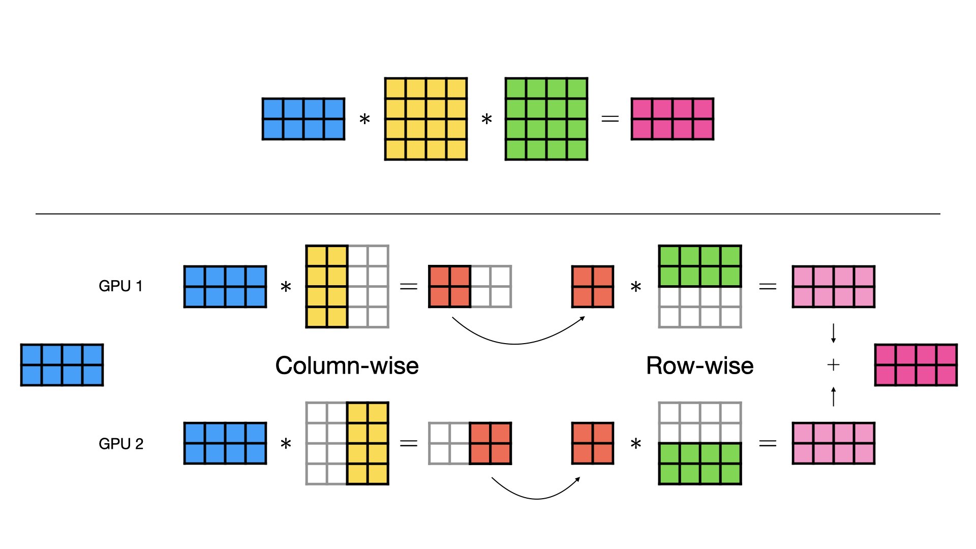
So as the model size gets bigger, the large K dimension (i.e., hidden_dim) hinders the GEMM process in the compute-bound FFN / MoE layers.

From NVIDIA official blog 1
PTX 9.4 docs mention the register descriptor tcgen05 MMA instruction now contains a bit indicating the K size in position 29.
For
.kind::f16,.kind::tf32,.kind:f8f6f4:
- Bit 29 for K dimension is valid for architecture sm_107f or higher in the same family. 2
For supported dtypes, the number of MMA K-iterations can be reduced, thus Rubin is able to provide higher overall throughput in the same instruction cycles.
Increased SFU for Softmax
Exponential throughput rises from Blackwell to Rubin 1:
| NVIDIA GPU platform | FP32 exponential throughput (per clk per SM) | BF16 / FP16 exponential throughput (per clk per SM) |
|---|---|---|
| Blackwell | ||
| Blackwell Ultra | ||
| Rubin |
The exponential computation in Softmax has become the bottleneck of attention, so NVIDIA spent more hardware units here. Another potential solution mentioned in FA4 5 is harnessing both native EXP (SFU) and software-emulated EXP (CUDA core) via Taylor expansion interleaved 6 to compute Softmax.
Fine-grained block-level PDL
Since Hopper, CUDA offers PDL (Programmatic Dependent Launch) capability to issue the second dependent kernel in advance so that the prologue can overlap over the final exit of the first kernel.
The first kernel informs its successor via cudaTriggerProgrammaticLaunchCompletion, and the second one firstly conducts some independent prologue then waits for the signal by cudaGridDependencySynchronize.

Block-level PDL.
Rubin extends this ability at a finer-grained level: the block level. Now each CTA in the second kernel can start immediately once the corresponding dependent blocks (CTAs) have released the flag.
This sounds more like the concept of MegaKernel, with this finer-grained PDL, it seems that we can achieve the goal of MegaKernel without messing the codes across the logic boundary.
In-flight TMA descriptor update
Currently (Hopper / Blackwell), to patch the TMA descriptor at the device side, we have to update a series of metadata in shared memory with additional memory barrier synchronization cost, like the following pseudo PTXs 2:
.global .align 128 .b8 gTensorMap[128];   // host-initialized descriptor
.shared .align 128 .b8 sTensorMap[128];

// 1. stage the 128 B descriptor into shared memory
cp.async.bulk.shared::cluster.global.mbarrier::complete_tx::bytes
    [sTensorMap], [gTensorMap], 128, [mbar];
// ... wait on mbar ...

// 2. patch the per-expert fields in place
tensormap.replace.tile.global_address.shared::cta.b1024.b64  [sTensorMap], newAddr;
tensormap.replace.tile.global_dim.shared::cta.b1024.b32      [sTensorMap], 0, newDim;
tensormap.replace.tile.global_stride.shared::cta.b1024.b64   [sTensorMap], 0, newStride;

// 3. copy back to global memory, releasing to the tensormap proxy
tensormap.cp_fenceproxy.global.shared::cta.tensormap::generic.release.gpu.sync.aligned
    [gTensorMap], [sTensorMap], 128;

// 4. acquire in the tensormap proxy before any TMA unit reads it
fence.proxy.tensormap::generic.acquire.gpu [gTensorMap], 128;

// 5. the descriptor is now consumable
cp.async.bulk.tensor.2d.shared::cluster.global.tile
    [sMem], [gTensorMap, {x, y}], [mbar];
Or there is a corresponding series of CuTe DSL tensormap manager APIs:
tensormap_manager = utils.TensorMapManager(
    utils.TensorMapUpdateMode.SMEM,      # or .GMEM
    bytes_per_tensormap,                 # 128
)
a_ptr = tensormap_manager.get_tensormap_ptr(tensormaps[(wsp_idx, 0, None)].iterator)

tensormap_manager.init_tensormap_from_atom(tma_atom_a, a_init_ptr, tma_warp_id)
tensormap_manager.fence_tensormap_initialization()

tensormap_manager.update_tensormap(
    (real_tensor_a, real_tensor_b),      # new gmem tensors for this group
    (tma_atom_a, tma_atom_b),
    (a_ptr, b_ptr),                      # gmem descriptor slots
    tma_warp_id,
    (a_smem_ptr, b_smem_ptr),
)
tensormap_manager.fence_tensormap_update(a_ptr)
Therefore, updating the TMA descriptor inside kernel hinders the end-to-end performance for latency-sensitive cases, e.g., a kernel in MoE layer processes multiple experts whose weights are located in different GMEM addresses.

Shared TMA descriptor via in-flight metadata update 1.
Since Rubin, CUDA supports inline override for some fields of the tensormap struct while sharing other common fields.
PTX ISA 9.4 adds the .override::global_address and .override_attribute qualifiers (requiring sm_107f) to:
cp.async.bulk.tensorcp.reduce.async.bulk.tensorcp.async.bulk.prefetch.tensor
Note that all experts of the MoE layer basically share the same shape, stride and dtype, with only the base memory address varying.
The overriding values are passed as extra operands right after tensorMap, so the descriptor itself stays untouched.
This could be combined with another feature introduced in Rubin: L2 cache control. Since Ampere, NVIDIA allows kernel authors to specify L2 cache line residual hints for normal LD instructions 7:
.ca: cache at all levels.cg: cache at L2, not L1.cs: cache streaming, evict-first policy in L1 and L2.lu: last use, acting like.cson global address space.cv: bypass cache
Rubin supports some of these cache residual hints by introducing qualifiers to cp.async.bulk.prefetch{.tensor} and applypriority.async.bulk{.tensor} instructions.
PTX 9.4 exposes them through a .level::eviction_priority qualifier on the bulk prefetch instructions, plus a pair of new applypriority.async.bulk instructions to apply the policy on a certain memory range, all requiring sm_107f 2:
// prefetch into L2 and pin the lines
cp.async.bulk.prefetch.tensor.dim.L2.src{.load_mode}{.level::eviction_priority}
    [tensorMap, tensorCoords]{, im2colInfo};
cp.async.bulk.prefetch.L2.src{.level::eviction_priority}   [srcMem], size;

.level::eviction_priority = { .L2::evict_last }

// retag resident lines once they are no longer worth keeping
applypriority.async.bulk.tensor.dim{.src}.completion_mechanism{.load_mode}
    .level::eviction_priority   [tensorMap, tensorCoords]{, im2colInfo};
applypriority.async.bulk{.src}.completion_mechanism.level::eviction_priority   [a], size;

.level::eviction_priority = { .L2::evict_normal }
Take MoE layer as example again, if all tokens for an expert have finished execution, the kernel can mark it as "last used".
ACK-free GIN by counted writes

Hardware-supported counter-based peer write.
CUDA / NCCL now supports network operations from the device 8. To inform the peer side that the transmission has finished, the sender side has to launch another flag write to peer memory with release semantic.
Rubin now supports a hardware-based counter that records the number of bytes the device receives across the NVLink. Once the counted bytes have reached the total bytes, the receiver can answer the consumer polls without the atomic flag write from the sender. This is very similar to the TMA-based async memory loading.
FP8 GEMM B-LUT
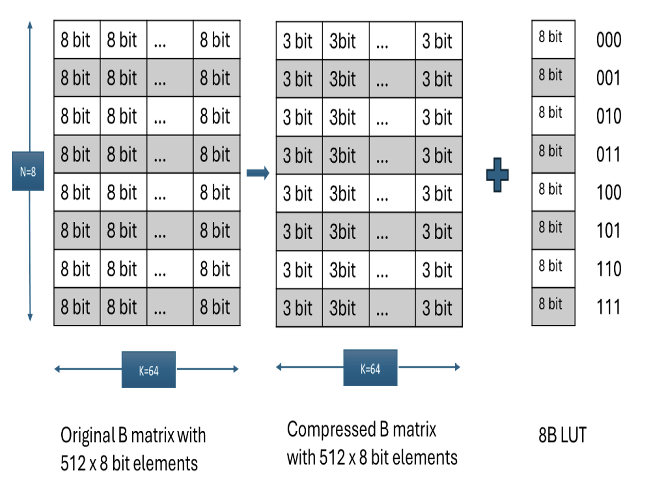
From "Figure 280" in https://docs.nvidia.com/cuda/developer-preview/13.4/pdf/ptx_isa_9.4.pdf
Rubin also supports FP8 GEMM with the pre-compressed matrix B, where TMEM stores the 8-bit pre-compressed B values (acting like a LUT) with capacity equal to 8, indexed by 3 bits ().
PTX 9.4 for Rubin adds a new .decompress::lut::b qualifier for the tcgen05.mma instruction: if specified, the tensor core will read 48 bytes from SMEM and leverage the first or second half of them ( bytes) as the LUT for MMA.
Vera: the CPU on the other side of NVLink-C2C
NVIDIA presented the Vera CPU at Hot Chips 2026 9, which is the host part paired with Rubin in the NVL72 rack. Unlike Grace, which was built from off-the-shelf Neoverse V2 cores, Vera uses NVIDIA's own Olympus core. This is the first NVIDIA-designed Arm core for servers, so the microarchitecture details are worth a closer look than the usual generation-over-generation spec bump.
Olympus core microarchitecture
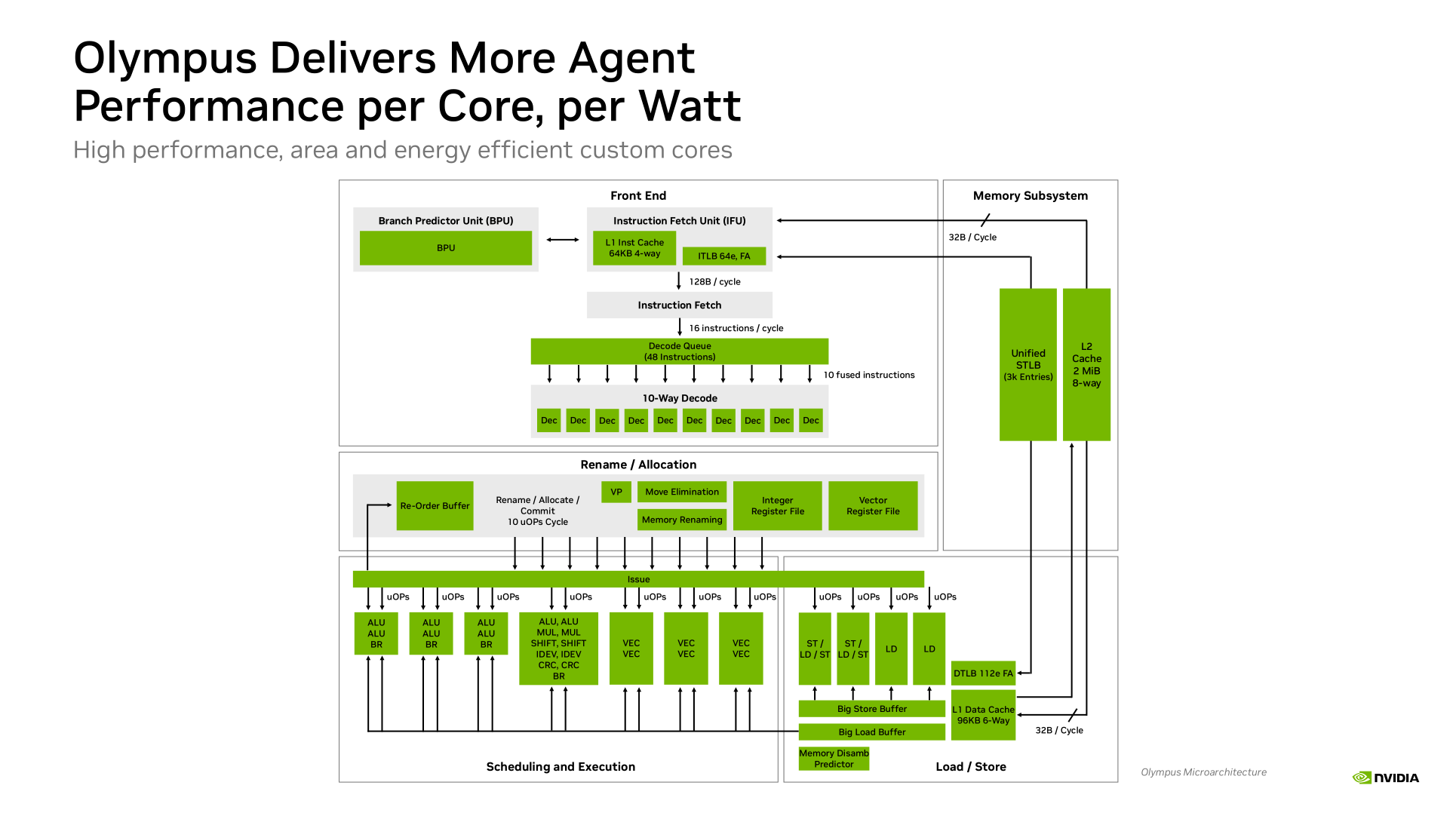
Olympus core block diagram 9.
The front end fetches 128 B per cycle from a 64 KB 4-way L1 instruction cache backed by a 64-entry fully-associative ITLB, delivering 16 instructions per cycle into a 48-entry decode queue. Decode is 10-wide and emits 10 fused instructions, and rename / allocate / commit also runs at 10 uOPs per cycle with move elimination and memory renaming. For reference, Neoverse V2 in Grace is 8-wide at rename, and current x86 server cores sit in the 6-8 range, so the 10-wide pipeline is genuinely at the wide end of shipping server cores.
The execution side has four integer clusters (three of ALU, ALU, BR plus one adding MUL, SHIFT, IDEV, CRC) and three 2-wide vector pipes.
Load / store provides two ST / LD-ST ports plus two dedicated LD ports against a 96 KB 6-way L1 data cache, a 112-entry fully-associative DTLB, and a memory disambiguation predictor feeding the big load / store buffers.
Each core owns a 2 MiB 8-way L2 and a 3k-entry unified STLB, with 32 B/cycle in each direction between L2 and the L1 caches.
Statically partitioned spatial multithreading
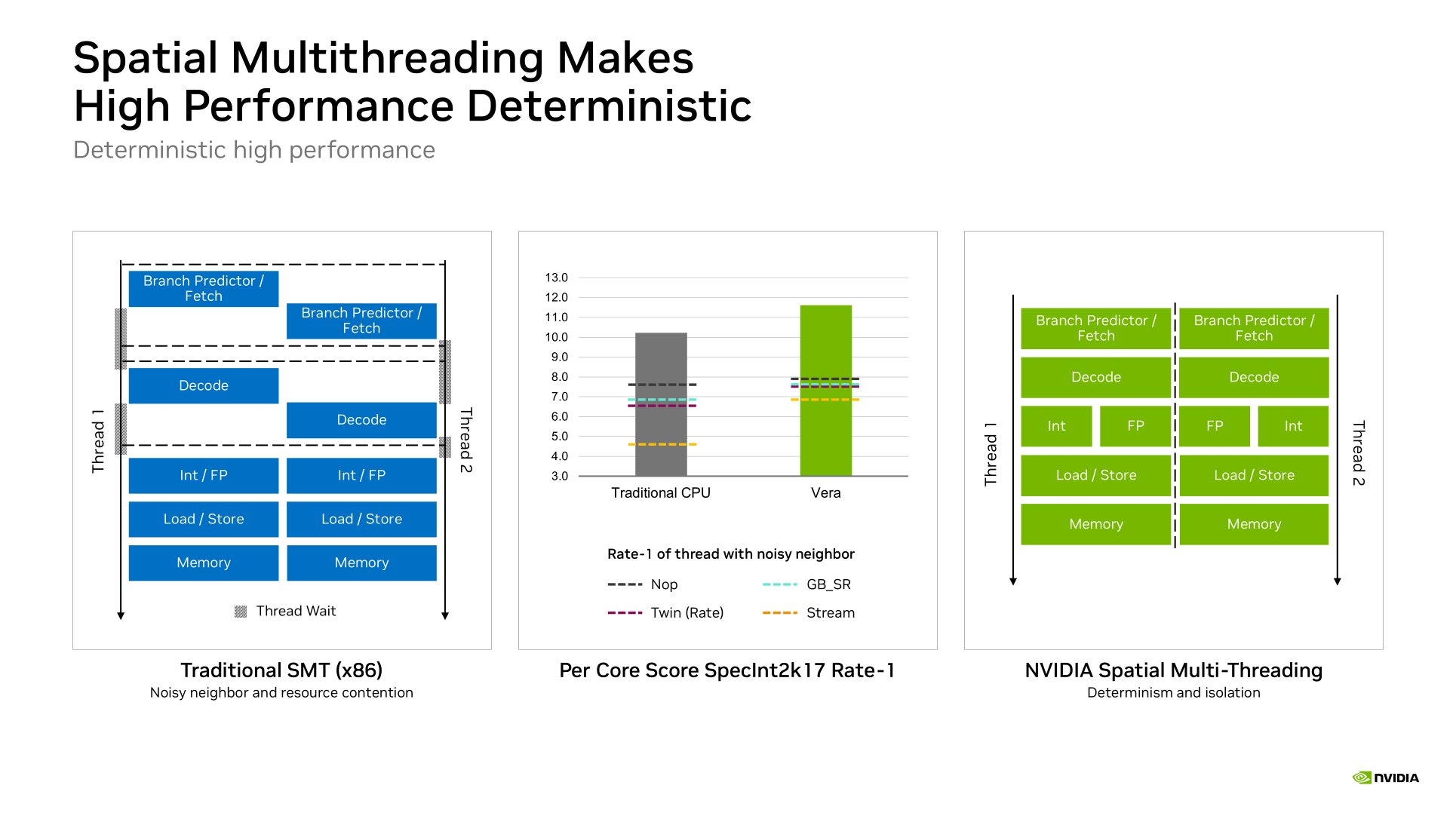
Spatial multithreading versus traditional SMT 9.
Olympus runs two threads per core (88 cores, 176 threads), but not through classic SMT. Instead of letting both threads compete for the same issue slots and buffers, the core statically partitions the front end, integer / FP pipes, load / store, and memory resources into two halves, one per thread. NVIDIA calls this spatial multithreading.
Six dies and the coherency fabric
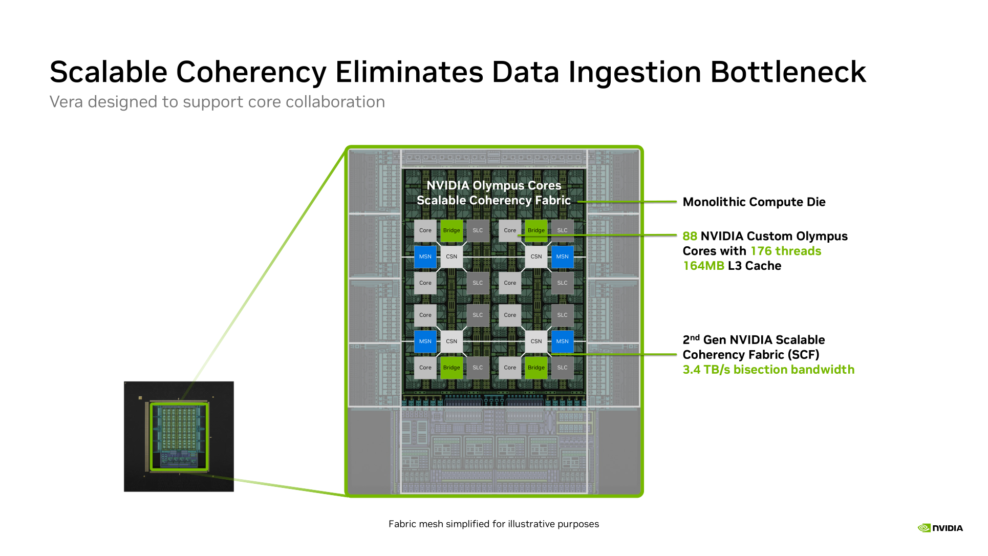
Vera die layout and the 2nd-gen Scalable Coherency Fabric 9.
Vera needed more silicon than one reticle-limited die, so it is split into 6 dies on a single interposer: the compute die stays monolithic, while the memory controllers and system I/O move to their own chiplets. Keeping all 88 cores on one die avoids the cross-die coherency penalty that multi-CCD designs pay, and pushes the disaggregation to the parts that tolerate latency (memory PHY and I/O).
The mesh is the 2nd-generation Scalable Coherency Fabric, with 3.4 TB/s of bisection bandwidth over a grid of core tiles, SLC slices (164 MB L3 in total), CSN switch nodes, MSN memory-side nodes, and bridge tiles to the chiplets.
LPDDR5X instead of DDR5
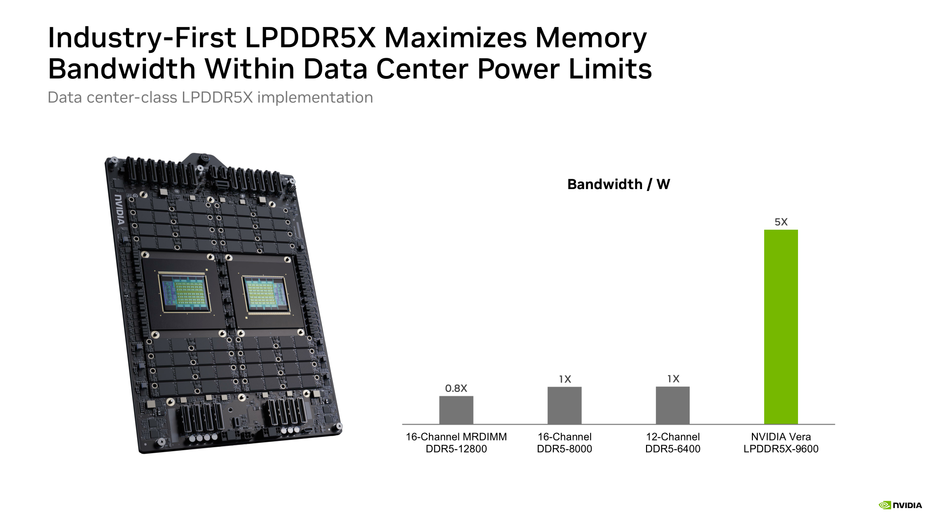
Data-center LPDDR5X-9600 subsystem 9.
Eight 128-bit LPDDR5X-9600 controllers give 1.5 TB of SOCAMM capacity at 1.2 TB/s. Grace topped out at 480 GB and around 500 GB/s, so this is roughly the capacity and the bandwidth.
The bar chart compares bandwidth per watt rather than absolute bandwidth, which is the honest framing here: the point of LPDDR5X is that the pJ/bit is low enough to fit a 1.2 TB/s memory subsystem inside the power budget left over after the GPUs take their share. A 16-channel MRDIMM DDR5-12800 configuration can reach comparable raw bandwidth, it just costs far more watts to do so. The trade-off, which the slide does not mention, is that SOCAMM modules are soldered-module class parts, so capacity is fixed at build time.
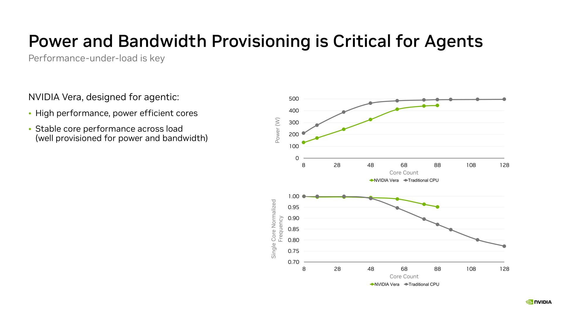
Package power and single-core frequency versus active core count 9.
The power slide is the only place a package-level number leaks: Vera lands somewhere below 450 W with all 88 cores active, while the anonymous "traditional CPU" baseline saturates near 500 W well before its 128 cores are busy. More useful is the lower curve, where Vera holds about 0.95 normalized single-core frequency at 88 active cores against roughly 0.87 for the baseline at the same count. That is what "well provisioned for power and bandwidth" actually means: less all-core frequency droop, so per-thread latency does not degrade as the box fills up.
Off-die bandwidth and I/O
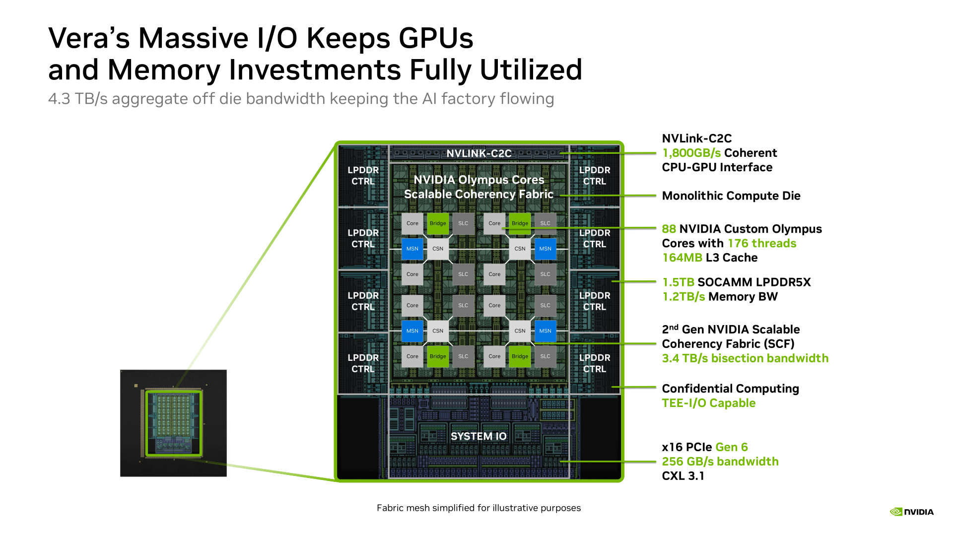
Vera off-die interfaces, totalling 4.3 TB/s 9.
The three off-die paths are NVLink-C2C at 1.8 TB/s coherent to Rubin (matching the Rubin-side number in the table above), the LPDDR5X controllers at 1.2 TB/s, and the system I/O die with 96 lanes of PCIe Gen 6 / CXL 3.1 at 256 GB/s per x16 link. NVIDIA totals these at 4.3 TB/s of aggregate off-die bandwidth. The PCIe lanes mostly go to ConnectX NICs rather than to accelerators, since the GPUs hang off NVLink-C2C instead. The same C2C interface can also connect two Vera chips for a 2P CPU-only server.
Footnotes
-
NVIDIA, Inside the NVIDIA Rubin GPU Architecture, for the Rubin SM count, NVFP4 dense throughput, HBM4 capacity and bandwidth, and the NVLink 6 and NVLink-C2C figures. ↩ ↩2 ↩3 ↩4
-
NVIDIA, Parallel Thread Execution ISA 9.4. ↩ ↩2 ↩3 ↩4
-
Rubin SXM spec sheet, for the Rubin FP8/FP6, BF16/FP16, FP32 and FP64 rates. The TDP and the SM count increase are corroborated by SemiAnalysis, Vera Rubin - Extreme Co-Design. ↩
-
Blackwell B200 figures from Comparing NVIDIA Tensor Core GPUs. The B300 FP64 figure is from Fifteen Years of FP64 Segmentation. ↩
-
https://docs.nvidia.com/cuda/developer-preview/13.4/parallel-thread-execution/index.html#cache-operators ↩
-
GIN https://docs.nvidia.com/deeplearning/nccl/user-guide/docs/usage/deviceapi.html ↩
-
ServeTheHome, NVIDIA Vera CPU at Hot Chips 2026, live coverage of the Hot Chips 2026 Vera talk; the slide numbers quoted here are read off the published slide images. ↩ ↩2 ↩3 ↩4 ↩5 ↩6 ↩7